

Application Notes for: Microwave Phase Shifters, IQ Vector Modulators & Frequency Translators
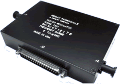
The Model 7218 is the latest addition to the family of high performance I.Q. Vector Modulators. Its broadband capability is ideally suited for today’s more demanding and complex Electronic Warfare systems. The Model 7218 covers a frequency range of 2 to 18 GHz, is capable of a full 360 Degrees phase control and a minimum of 20 dB amplitude control. Response time is 1 microsecond, maximum. Digital control is accomplished by two 12 bit TTL inputs, for I and Q channels, which provide for high precision calibration of phase and amplitude. Operation is guaranteed to be monotonic.
- Broad Frequency range – 2 to 18 GHz
- Simultaneous control of phase and amplitude
- Digitally programmable – 12 Bits for both I & Q
- High Speed
- Guaranteed monotonic
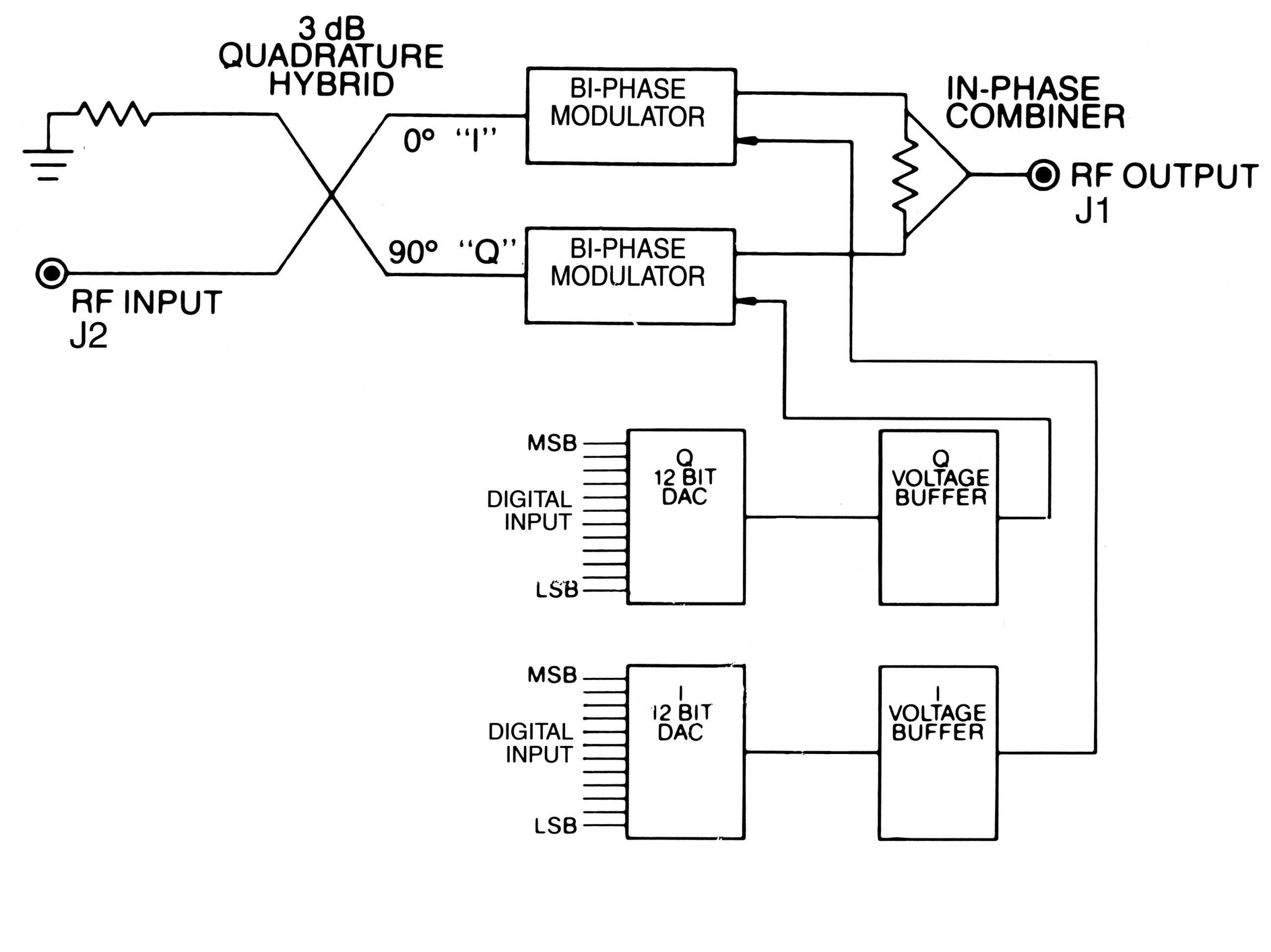
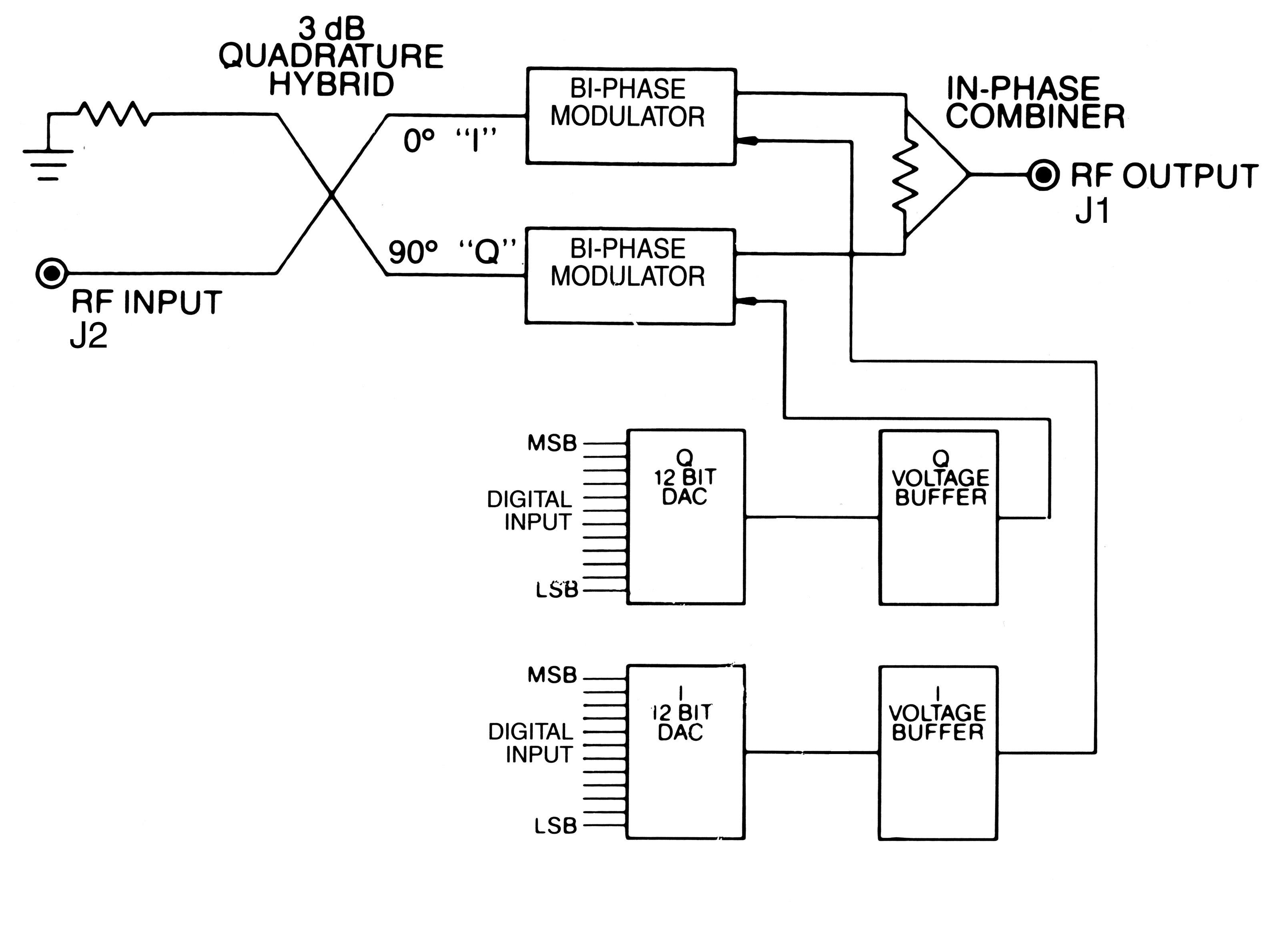
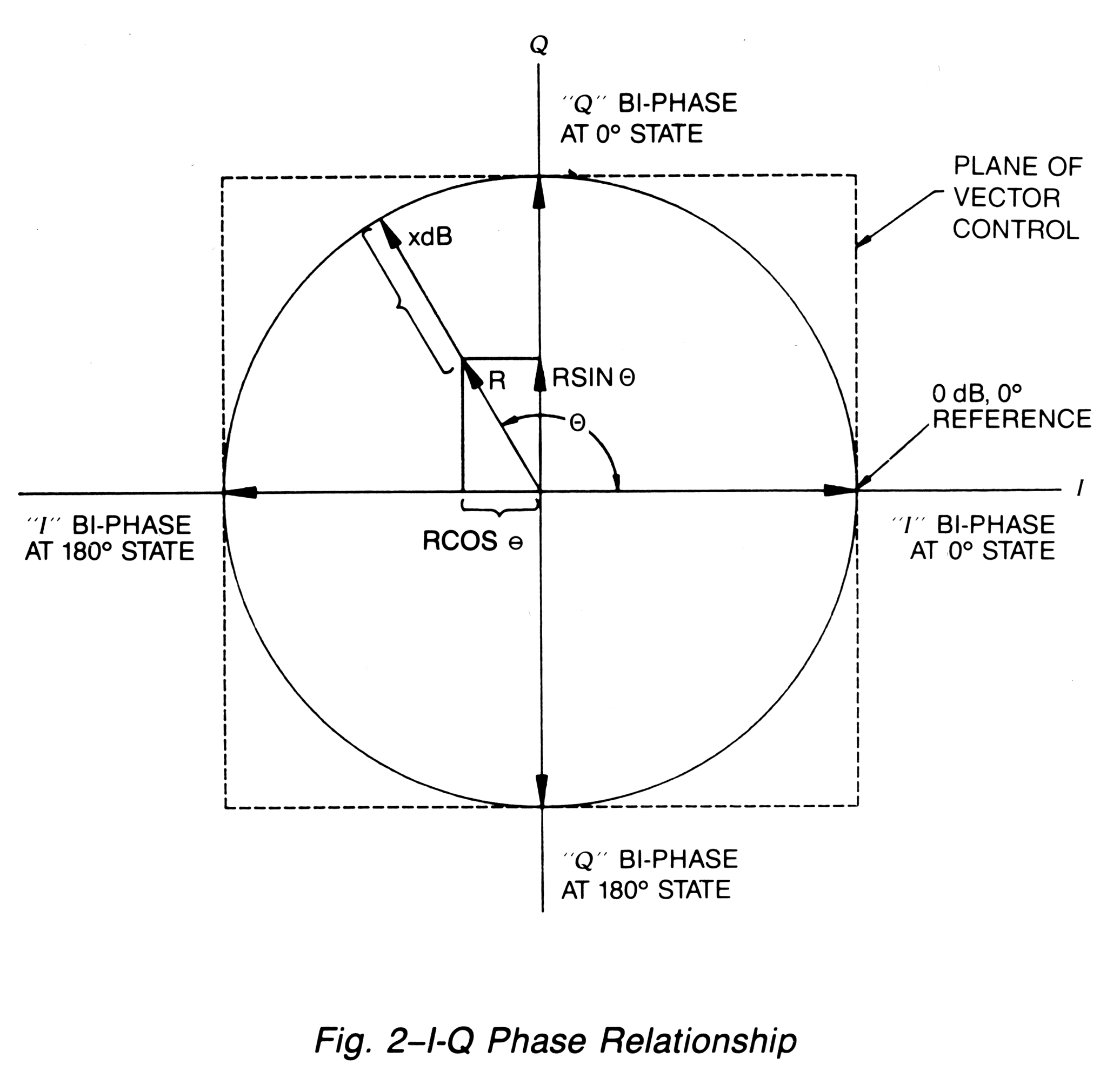
The block diagram of the microwave I-Q Vector Modulator is shown in Figure 1. An RF signal incident on a 3 dB quadrature hybrid is divided into two equal outputs, with a 90° phase difference between them. The in-phase, or 0°, channel is designated the I channel and the Quadrature, or 90°, channel is designated the Q channel. Each signal passes through a biphase modulator which sets the 0° or 180° state and the attenuation level for both the I and Q paths. The outputs of the I and Q path are combined to yield the resultant vector which may fall anywhere within the bounded area shown in Figure 2. Any signal applied to the I/Q Vector Modulator can be shifted in phase and adjusted in amplitude by applying the following relationships:
- Let the desired attenuation level = X dB and the desired phase shift = θ° (with respect to 0 dB and 0° reference states).
- The normalized output voltage magnitude is given by: |V| = 10^(x/20).
- The values of the I and Q attenuator control inputs are then expressed as:
I = V cos θ
and
Q = V sin θ
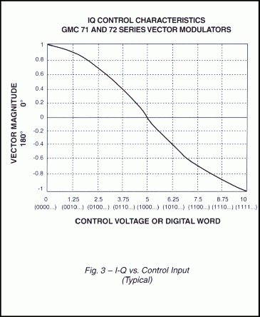
Figure 3 shows the nominal value of I and Q vs. either digital word (Series 71) or analog voltage (Series 72). Thus, to achieve an attenuation level of 3 dB with a phase offset of 112.5° (with respect to 0 dB and 0° reference states) the values of I and Q can be calculated as follows:
|V| = 10^(-3/20) = 0.707
I = 0.707 cos (112.5°) =–0.27
Q = 0.707 sin (112.5°) =+0.65
From Figure 3, the control inputs to yield the desired amplitude and phase are approximately:
| Analog Units (72 Series) | Digital Units (71 Series) |
|---|---|
| I = 5.78 volts | 100101000000 |
| Q = 2.84 volts | 010010001011 |
While these values for I and Q will yield an output signal whose amplitude and phase are close to the nominal values over the entire operating frequency range of the vector modulator, the use of an iterative measurement procedure will determine the I and Q inputs which exactly define the desired parameter at any selected frequency.
| PARAMETER | SPECIFICATION | |
| OPERATING FREQUENCY RANGE | 2.0 – 18.0 GHz | |
| Band 1 | 2 – 6 GHz | |
| Band 2 | 6 – 18 GHz | |
| Band Switching Speed,max | 250 nanoseconds | |
| INSERTION LOSS (MAX) | 16 dB | |
| VSWR (MAX) | 2.2:1 | |
| POWER HANDLING CAPABILITY | ||
| Without performance degradation | +20 dBm | |
| Survival | 1 W | |
| ABSOLUTE INSERTION PHASE ACCURACY VS. FREQUENCY (MAX) | ±15o (in each band) | |
| VARIATION OF PHASE VS. TEMPERATURE (MAX) | ±0.1 deg./ oC | |
| ATTENUATION RANGE (MIN) | 20 dB | |
| VARIATION OF AMPLITUDE VS. TEMPERATURE (MAX) | 0.02 dB/ oC | |
| RESPONSE TIME (MAX) | 1.0 µsec | |
| POWER SUPPLY | +5 V ±2% @ 200 mA, max. +12 to +15V @ 150 mA, max. -5.2 V ±2% @ 400 mA, max. -12 to -15V @ 150 mA, max |
|
| MONOTONICITY | GUARANTEED | |
| Control INPUT | 12 BIT TTL FOR BOTH I & Q INPUTS | |
| CONNECTORS | ||
| RF Input/output | SMA Female, 2X | |
| Control/Power | Cannon DC-37P or Equivalent | |
| TEMPERATURE RANGE | ||
| Operating | -55 oC to +85 oC | |
| Storage | -65 oC to +125 oC | |
RECOMMENDED SEQUENCE OF POWERING THE SUPPLIES
| 1. | Set command lines to logic level “0”. |
| 2. | Turn on the -12 to -15V power supply. |
| 3. | Turn on the +12 to +15V power supply. |
| 4. | Turn on the +5V power supply. |
| 5. | Set command lines to logic level “1”. |
| 6. | Now you can start to work (if you want for example zero phase, set again all control lines to “0”) |
| Mating power/control connector |
| OPTION No. | DESCRIPTION |
| G09 | Guaranteed to meet Environmental Ratings |
| G12 | RoHS Compliant |
| G18 | REACH Compliant |
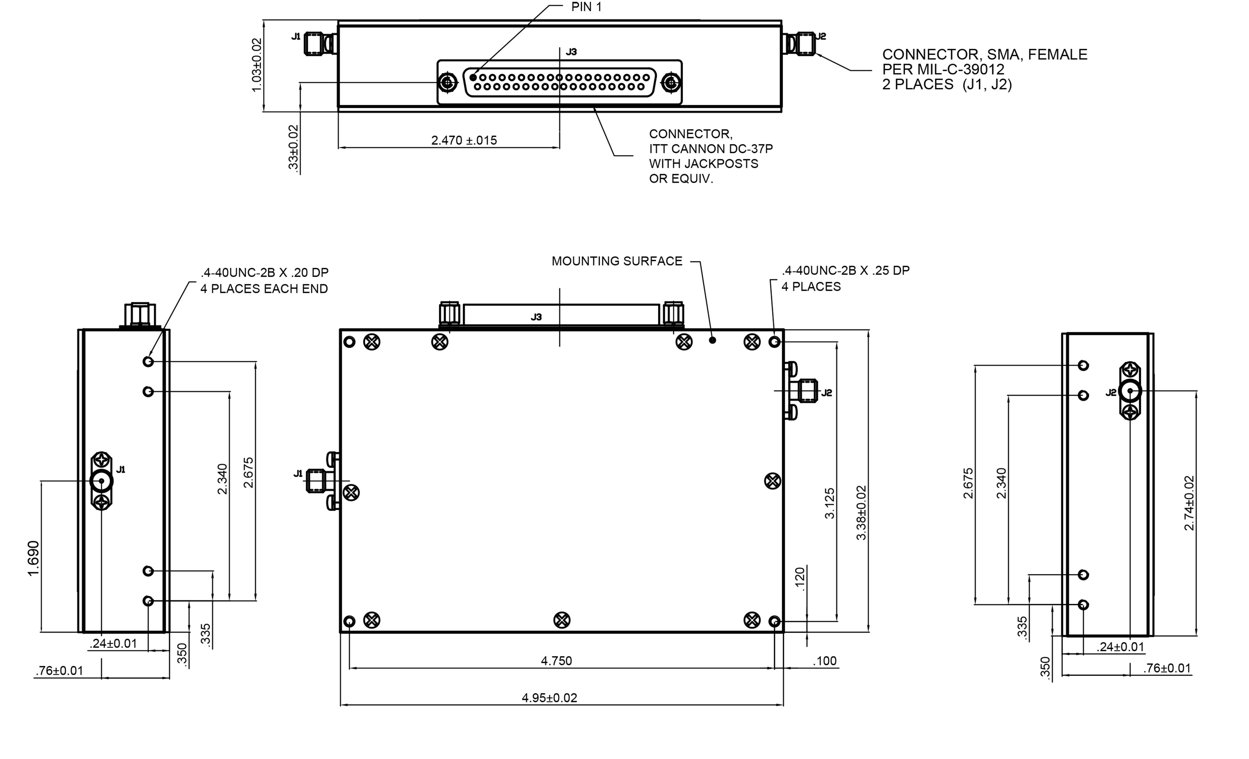
Dimensions are stated in inches (mm). Tolerances, unless otherwise indicated: .XX ±.02; .XXX ±.008
|
||||||||||||||||||||||||||||||||||||||||||||||||||||||||||||||||||||||||||||||||||||
- BAND SELECT:
Band 1 (2 to 6 GHz) – Apply TTL 0 to Pin 7 AND/OR Pin 29; Apply TTL 1 to Pins 31 AND 33.
Band 2 (6 to 18 GHz) – Apply TTL 0 to Pin 31 AND/OR Pin 33. Apply TTL 1 to Pins 7 AND 29. - ISOLATION State: Apply TTL 1 to Pins 7, 29, 31 AND 33. At this state unit is reflective (VSWR is undetermined).
- Control functions for other TTL combinations of Pins 7, 29, 31 and 33 are invalid states.