

pplication Notes for RF Switches
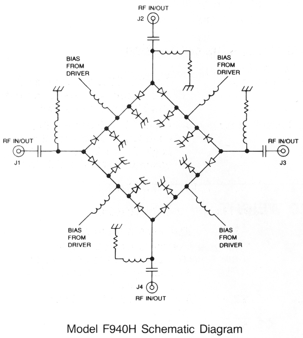
Model F940H is a high-performance broadband transfer switch that operates over the full instantaneous bandwidth of 0.5 to 18 GHz with ON and OFF times of 30 ns. Design features include an integrated circuit assembly of PIN diodes mounted in a microstrip transmission line as well as a resistive bias line that contributes to the broadband low-loss performance. The circuit configuration of the Model F940H is shown below.
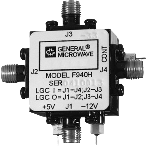
The Model F940H is equipped with an integrated driver that is powered by +5 and –12 volt supplies. The proper currents required to switch the ports ON or OFF are provided by the driver, which is controlled by external logic signals.
- Frequency range: 0.5 to 18 GHz
- Low VSWR and Insertion loss
- Isolation: up to 60 dB
- Small size, light weight
PERFORMANCE CHARACTERISTICS
| CHARACTERISTIC | FREQUENCY (GHz) | ||
|---|---|---|---|
| 0.5 to 8.0 |
8.0 to 12.4 |
12.4 to 18.0 |
|
|
|
60 2.0 1.75 |
55 2.5 1.75 |
50 3.5 2.0 |
| Switching Time | |||||||||||||
| 30 ns max. | |||||||||||||
| 30 ns max. | |||||||||||||
| Power Handling Capability | |||||||||||||
| 500 mW cw or peak | |||||||||||||
| 1W average, 75W peak (1 µsec max. pulse width) | |||||||||||||
| +5V ±5%, 60 mA | |||||||||||||
| –12V ±5%, 75 mA | |||||||||||||
| Schottky TTL, two unit loads. (A unit load is 2 mA sink current and 50 µA source current.)
|
|||||||||||||
| Logic “0” (-0.3 to +0.8V) connects to J1 to J2 and J3 to J4 Logic “1” (+2.0 to +5.0V) connects to J1 to J4 and J2 to J3 |
|||||||||||||
| OPTION (G09) ENVIRONMENTAL RATINGS | |||||||||||||
| –54°C to +110°C | |||||||||||||
| –65°C to +125°C | |||||||||||||
| MIL-STD-202F, Method 103B, Cond. B (96 hrs. at 95%) | |||||||||||||
| MIL-STD-202F, Method 213B, Cond. B (75G, 6 msec) | |||||||||||||
| MIL-STD-202F, Method 204D, Cond. B (.06″ double amplitude or 15G, whichever is less) | |||||||||||||
| MIL-STD-202F, Method 105C, Cond. B (50,000 ft.) | |||||||||||||
| MIL-STD-202F, Method 107D Cond. A, 5 cycles | |||||||||||||
| AVAILABLE OPTIONS | ||
| Option No. | Description | |
| 7 | SMA male RF connectors | |
| 9 | Inverse control logic; logic “0” connects J1 to J4 and J2 to J3, and logic “1” onnects J1 to J2 and J3 to J4 | |
| 33 | EMI filter solder-type control terminal | |
| 48 | +5V, –15V operation | |
| 64A | SMB male control connector | |
| G09 | Guaranteed to meet Environmental Ratings | |
| G12 | RoHS Compliant | |
| G18 | REACH Compliant | |
DIMENSIONS AND WEIGHT
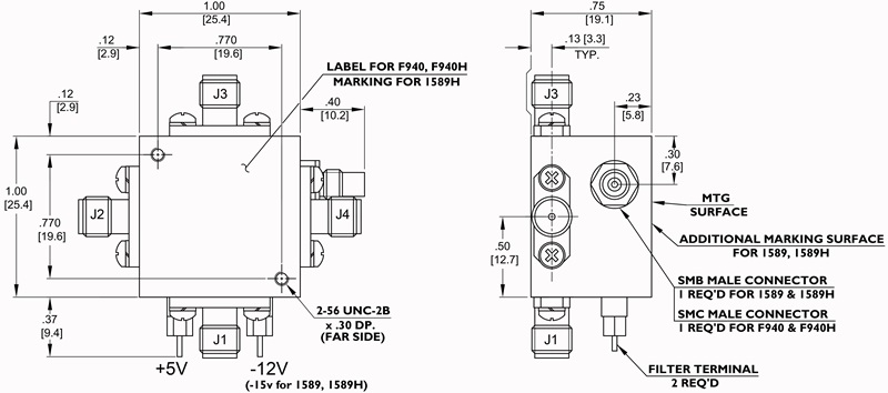
Dimensions in mm (Inches) Tolerances, unless otherwise indicated: .XX ±.02; .XXX ±.005